| CPC H01L 25/0657 (2013.01) [H01L 24/03 (2013.01); H01L 24/05 (2013.01); H01L 24/49 (2013.01); H01L 29/41741 (2013.01); H01L 2224/0231 (2013.01); H01L 2224/0233 (2013.01); H01L 2224/49097 (2013.01); H01L 2924/1438 (2013.01); H01L 2924/15321 (2013.01)] | 17 Claims |
|
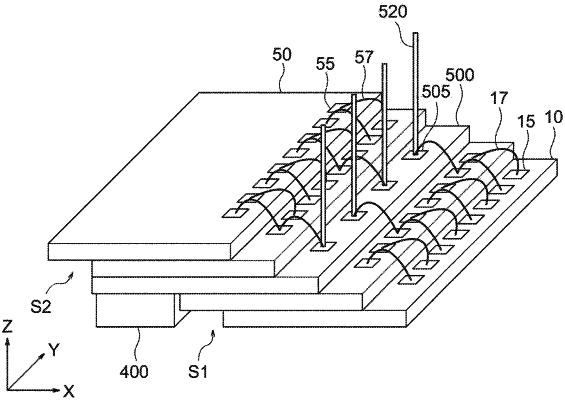
1. A semiconductor device comprising:
a first stacked body including a plurality of first semiconductor chips stacked along a first direction, each of the first semiconductor chips being offset from the other first semiconductor chips along a second direction perpendicular to the first direction;
a first columnar electrode connected to an electrode pad of the first stacked body, and extending in the first direction;
a second stacked body including a plurality of second semiconductor chips stacked along the first direction, each of the second semiconductor chips being offset from the other second semiconductor chips along the second direction, the second stacked body having a height larger than the first stacked body and overlap at least a portion of the first stacked body when viewed from the top; and
a second columnar electrode connected to an electrode pad of the second stacked body, and extending in the first direction.
|