| CPC H01L 25/0657 (2013.01) [H01L 23/16 (2013.01); H01L 23/31 (2013.01); H01L 23/5386 (2013.01)] | 20 Claims |
|
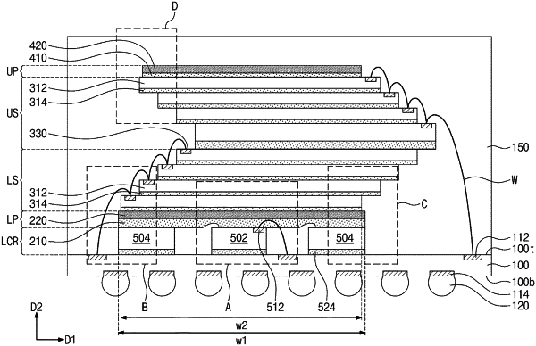
1. A semiconductor package comprising:
a chip stack comprising semiconductor chips vertically stacked on a substrate in a first direction perpendicular to a top surface of the substrate;
pillars between the substrate and the chip stack;
an adhesive layer on a bottom surface of a lowermost semiconductor chip of the semiconductor chips;
a first lower protective layer between the adhesive layer and the pillars;
a second lower protective layer between the first lower protective layer and the adhesive layer; and
a mold layer covering the chip stack and filling a space between the pillars,
wherein a thickness of the second lower protective layer in the first direction is greater than a thickness of the adhesive layer in the first direction.
|
|
13. A semiconductor package comprising:
a chip stack comprising semiconductor chips vertically stacked on a substrate in a first direction perpendicular to a top surface of the substrate, the chip stack comprising a first semiconductor chip located at a lowest level of the semiconductor chips;
pillars between the substrate and the first semiconductor chip;
an adhesive layer on a bottom surface of the first semiconductor chip;
a first lower protective layer between the adhesive layer and the pillars; and
a second lower protective layer between the first lower protective layer and the adhesive layer,
wherein the first semiconductor chip has first sidewalls opposite to each other in a second direction parallel to the top surface of the substrate,
wherein the second lower protective layer has second sidewalls opposite to each other in the second direction, and
wherein the second sidewalls are offset from the first sidewalls in the second direction.
|
|
18. A semiconductor package comprising:
a chip stack comprising semiconductor chips vertically stacked on a substrate in a first direction perpendicular to a top surface of the substrate, the chip stack comprising a first semiconductor chip located at a lowest level and a second semiconductor chip located at a highest level of the semiconductor chips;
upper conductive pads on a top surface of the substrate;
lower conductive pads on a bottom surface of the substrate;
pillars between the top surface of the substrate and the chip stack, wherein at least one of the pillars comprises a lower semiconductor chip electrically connected to a corresponding one of the upper conductive pads;
an adhesive layer on a bottom surface of the first semiconductor chip;
a first lower protective layer between the adhesive layer and the pillars;
a second lower protective layer between the first lower protective layer and the adhesive layer;
a first upper protective layer on the second semiconductor chip;
a second upper protective layer on the first upper protective layer; and
a mold layer covering the chip stack and filling a space between the pillars,
wherein a thickness of the first upper protective layer in the first direction is less than a thickness of the second upper protective layer in the first direction.
|