| CPC H01L 25/0657 (2013.01) [H01L 23/3142 (2013.01); H01L 24/29 (2013.01); H01L 2224/94 (2013.01)] | 17 Claims |
|
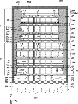
1. A semiconductor package, comprising:
a first semiconductor chip stack and a second semiconductor chip stack that are adjacent to each other,
wherein the first semiconductor chip stack includes a plurality of first semiconductor chips and a plurality of first adhesive layers,
wherein the second semiconductor chip stack includes a plurality of second semiconductor chips and a plurality of second adhesive layers,
wherein each of the first semiconductor chips includes a first cell region and a first scribe lane that has a rectangular annulus shape that surrounds the first cell region,
wherein each of the second semiconductor chips includes a second cell region and a second scribe lane that has a rectangular annulus shape that surrounds the second cell region,
wherein an area of the first scribe lane is greater than an area of the second scribe lane,
wherein the plurality of first adhesive layers and the plurality of second adhesive layers have the same coefficient of thermal expansion,
wherein each of the first semiconductor chips includes a first protective ring disposed between the first scribe lane and the first cell region,
wherein each of the second semiconductor chips includes a second protective ring disposed between the second scribe lane and the second cell region, and
wherein a spacing distance between the first protective ring and an adjacent lateral surface of each of the first semiconductor chips is greater than a spacing distance between the second protective ring and an adjacent lateral surface of each of the second semiconductor chips.
|