| CPC H01L 25/0657 (2013.01) [H01L 21/78 (2013.01); H01L 24/08 (2013.01); H01L 24/80 (2013.01); H01L 25/18 (2013.01); H01L 25/50 (2013.01); H01L 2224/08145 (2013.01); H01L 2224/80895 (2013.01); H01L 2224/80896 (2013.01); H01L 2225/06524 (2013.01); H01L 2924/1431 (2013.01); H01L 2924/1436 (2013.01); H01L 2924/1437 (2013.01)] | 20 Claims |
|
1. A semiconductor device, comprising:
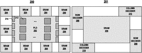
a first semiconductor structure comprising a programmable logic device, an array of static random-access memory (SRAM) cells, and a first bonding layer comprising a plurality of first bonding contacts, wherein the array of SRAM cells is located in a peripheral region of the first semiconductor structure surrounding the programmable logic device;
a second semiconductor structure comprising an array of dynamic random-access memory (DRAM) cells, a pad-out interconnect layer above the array of DRAM cells, a second bonding layer comprising a plurality of second bonding contacts, and at least one interconnect contact extending through the second semiconductor structure, wherein the at least one interconnect contact provides an electrical path between the pad-out interconnect layer and the second bonding layer; and
a bonding interface between the first bonding layer and the second bonding layer, wherein the first bonding contacts are in contact with the second bonding contacts at the bonding interface,
wherein the programmable logic device and array of SRAM cells are electrically connected to the array of DRAM cells through the first and second bonding contacts and the at least one interconnect contact.
|