| CPC H01L 25/0652 (2013.01) [H01L 21/6836 (2013.01); H01L 21/82 (2013.01); H01L 23/481 (2013.01); H01L 24/08 (2013.01); H01L 24/80 (2013.01); H01L 25/50 (2013.01); H01L 2221/68327 (2013.01); H01L 2224/08146 (2013.01); H01L 2224/80895 (2013.01); H01L 2224/80896 (2013.01); H01L 2225/06524 (2013.01); H01L 2225/06541 (2013.01); H01L 2225/06568 (2013.01); H01L 2225/06582 (2013.01)] | 20 Claims |
|
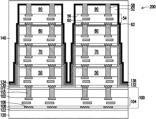
1. A method comprising:
bonding a first die to a package substrate, the first die comprising first vias disposed in a first substrate of the first die;
after bonding the first die to the package substrate, etching a backside of the first die such that top surfaces of the first vias extend above top surfaces of the first substrate;
conformally depositing a first dielectric film over the package substrate and the first die, the first dielectric film extending along sidewalls and the top surfaces of the first vias;
planarizing the first dielectric film to expose the top surfaces of the first vias; and
bonding a second die to the first die, the second die being bonded to the first dielectric film and the first vias.
|
|
8. A method comprising:
bonding a first die to a package substrate, the first die comprising a via extending through a substrate;
depositing a first dielectric film extending along a top surface of the package substrate, a top surface of the substrate, a top surface of the via, and sidewalls of the via;
removing the first dielectric film from the top surface of the via;
bonding a second die to the first dielectric film and the via; and
encapsulating the first die, the first dielectric film, and the second die with an encapsulant, wherein the encapsulant contacts the first dielectric film and a sidewall of the second die.
|
|
15. A method comprising:
providing a first die comprising a first via in a first substrate;
thinning a backside of the first substrate to expose the first via;
bonding a front-side of the first die opposite the backside of the first substrate to a package substrate;
depositing a first dielectric layer over the first die and the package substrate;
planarizing the first dielectric layer such that a top surface of the first dielectric layer is level with a top surface of the first via; and
encapsulating the first die and the first dielectric layer.
|