| CPC H01L 24/97 (2013.01) [H01L 21/6836 (2013.01); H01L 21/78 (2013.01); H01L 24/32 (2013.01); H01L 2221/68327 (2013.01); H01L 2221/68368 (2013.01); H01L 2224/32245 (2013.01); H01L 2224/95001 (2013.01)] | 7 Claims |
|
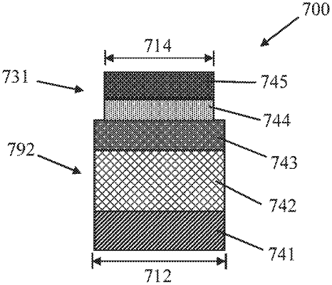
1. A wafer level chip scale semiconductor package comprising:
a device semiconductor layer comprising a plurality of metal electrodes disposed on a front surface of the device semiconductor;
a backside metallization layer attached to a back surface of the device semiconductor layer;
a metal layer attached through a film laminate layer to the backside metallization layer; and
a marking film coating layer overlaying the metal layer;
wherein each side surface of the backside metallization layer is coplanar with a corresponding side surface of the device semiconductor layer;
wherein each side surface of the metal layer is coplanar with a corresponding side surface of the film laminate layer; and
wherein a surface area of a back surface of the backside metallization layer is smaller than a surface area of a front surface of the metal layer.
|