| CPC H01L 24/80 (2013.01) [H01L 24/03 (2013.01); H01L 24/05 (2013.01); H01L 25/0657 (2013.01); H01L 25/50 (2013.01); H01L 2224/80031 (2013.01); H01L 2224/80345 (2013.01); H01L 2224/80895 (2013.01); H01L 2924/37001 (2013.01)] | 16 Claims |
|
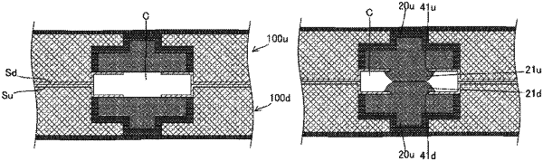
1. A semiconductor device, comprising:
a first substrate;
a second substrate;
a first insulating layer;
a second insulating layer, wherein a first portion of the first insulating layer is in contact with a first portion of the second insulating layer;
a first electrode;
a second electrode, wherein a first portion of the first electrode is in contact with a first portion of the second electrode;
a first recess between a second portion of the first electrode and a second portion of the second electrode; and
a first barrier metal film, wherein the first recess is between the first barrier metal film and the first portion of the first electrode.
|