| CPC H01L 24/80 (2013.01) [H01L 21/78 (2013.01); H01L 24/08 (2013.01); H01L 25/0657 (2013.01); H01L 25/50 (2013.01); H01L 2224/08145 (2013.01); H01L 2224/80006 (2013.01); H01L 2224/80895 (2013.01); H01L 2224/80896 (2013.01); H01L 2225/06541 (2013.01)] | 20 Claims |
|
1. A method comprising:
forming a first carrier comprising a blank silicon layer, and a surface layer over the blank silicon layer;
bonding a first wafer to the surface layer of the first carrier, wherein the first wafer comprises a semiconductor substrate, and a first plurality of through-vias extending into the semiconductor substrate;
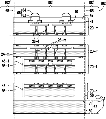
bonding a first plurality of chips over the first wafer, with gaps located between the first plurality of chips;
performing a gap-filling process to form gap-filling regions in the gaps;
bonding a second carrier onto the first plurality of chips and the gap-filling regions;
de-bonding the first carrier from the first wafer, wherein after the de-bonding the first carrier, the surface layer remains to be bonded to the first wafer; and
forming electrical connectors electrically connecting to conductive features in the first wafer, wherein the electrical connectors are electrically connected to the first plurality of chips through the first plurality of through-vias.
|