US 11,721,662 B2
Wafer bonding method and wafer bonding apparatus
Yun-Tai Shih, Changhua (TW); Ching-Hou Su, Hsinchu (TW); Chyi-Tsong Ni, Hsinchu (TW); I-Shi Wang, Taipei (TW); Jeng-Hao Lin, Chubei (TW); Kuan-Ming Pan, Hsinchu (TW); Jui-Mu Cho, Chupei (TW); and Wun-Kai Tsai, Yunlin (TW)
Assigned to TAIWAN SEMICONDUCTOR MANUFACTURING COMPANY, LTD., Hsinchu (TW)
Filed by TAIWAN SEMICONDUCTOR MANUFACTURING COMPANY, LTD., Hsinchu (TW)
Filed on Nov. 4, 2020, as Appl. No. 17/89,183.
Application 16/546,861 is a division of application No. 14/819,552, filed on Aug. 6, 2015, granted, now 10,396,054, issued on Aug. 27, 2019.
Application 14/819,552 is a division of application No. 13/267,336, filed on Oct. 6, 2011, granted, now 9,123,754, issued on Sep. 1, 2015.
Application 17/089,183 is a continuation of application No. 16/546,861, filed on Aug. 21, 2019, granted, now 10,847,490.
Prior Publication US 2021/0050324 A1, Feb. 18, 2021
This patent is subject to a terminal disclaimer.
Int. Cl. H01L 23/00 (2006.01); H01L 23/544 (2006.01); H01L 21/68 (2006.01); H01L 21/67 (2006.01)
CPC H01L 24/75 (2013.01) [H01L 21/67092 (2013.01); H01L 21/681 (2013.01); H01L 23/544 (2013.01); H01L 21/68 (2013.01); H01L 21/682 (2013.01); H01L 2223/54426 (2013.01); H01L 2224/75703 (2013.01); H01L 2224/75753 (2013.01); H01L 2224/75901 (2013.01); Y10T 29/49 (2015.01); Y10T 29/49002 (2015.01); Y10T 29/49131 (2015.01); Y10T 29/49764 (2015.01); Y10T 29/53022 (2015.01)] 20 Claims
OG exemplary drawing
 
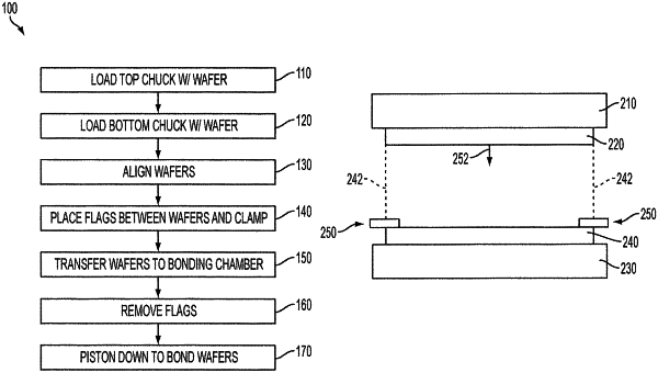
1. A method of aligning two wafers during a bonding process, the method comprising:
aligning a first wafer having a plurality of alignment markings with a second wafer having a plurality of alignment markings;
placing a plurality of flags between the first wafer and the second wafer;
detecting movement of the plurality of flags with respect to the first wafer and the second wafer using at least one sensor; and
determining whether the wafers remain aligned within an alignment tolerance based on the detected movement of the plurality of flags relative to the first wafer and the second wafer.