| CPC H01L 24/08 (2013.01) [H01L 22/20 (2013.01); H01L 24/80 (2013.01); H01L 25/0657 (2013.01); H01L 25/18 (2013.01); H01L 25/50 (2013.01); H01L 2224/08145 (2013.01); H01L 2224/80895 (2013.01); H01L 2224/80896 (2013.01); H01L 2224/80908 (2013.01); H01L 2225/06596 (2013.01); H01L 2924/1431 (2013.01); H01L 2924/14511 (2013.01)] | 20 Claims |
|
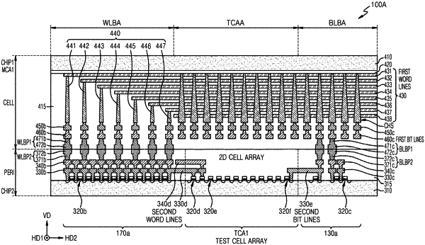
1. A memory device, comprising:
a memory chip including
a memory cell array connected to first word lines and first bit lines,
first word line bonding pads respectively connected to the first word lines, and
first bit line bonding pads respectively connected to the first bit lines; and
a peripheral circuit chip, wherein the peripheral circuit chip includes
a test cell array connected to second word lines and second bit lines,
second word line bonding pads respectively connected to the first word line bonding pads,
second bit line bonding pads respectively connected to the first bit line bonding pads, and
a peripheral circuit connected to
the second word line bonding pads and the second word lines, or
the second bit line bonding pads and the second bit lines,
wherein the memory cell array is disposed above the test cell array in a vertical direction.
|