| CPC H01L 24/06 (2013.01) [H01L 24/97 (2013.01); H01L 25/0655 (2013.01); H01L 2224/16245 (2013.01); H01L 2924/01029 (2013.01); H01L 2924/14 (2013.01)] | 18 Claims |
|
1. A method comprising:
attaching a plurality of semiconductor die to a temporary carrier substrate between copper pillars disposed on the temporary carrier substrate, each of the plurality of semiconductor die having a backside metal drain contact;
covering the plurality of semiconductor die and the copper pillars on the temporary carrier substrate with molding material;
backside grinding the molding material to expose first ends of the copper pillars and the backside metal drain contacts of the plurality of semiconductor die;
applying a first layer of conductive material to electrically connect the first ends of the copper pillars and backside metal drain contacts of the plurality of semiconductor die;
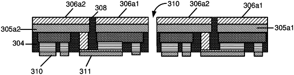
cutting grooves in the first layer of conductive material to isolate pairs of adjacent semiconductor dies of the plurality of semiconductor die to be contained in individual multi-chip module (MCM) packages, each pair of adjacent semiconductor die including a first semiconductor die and a second semiconductor die;
removing the temporary carrier substrate to expose second ends of the copper pillars in place in the molding material;
applying a second layer of conductive material to electrically connect the second ends of the copper pillars and source contacts of the pairs of adjacent semiconductor die; and
singulating the individual MCM packages, each individual MCM package including the first semiconductor die and the second semiconductor die of a pair of adjacent semiconductor die with a source of the first semiconductor die connected to a drain of the second semiconductor die via one of the copper pillars left in place in the molding material.
|