US 11,721,649 B2
Microelectronic assemblies
Adel A. Elsherbini, Tempe, AZ (US); Patrick Morrow, Portland, OR (US); Henning Braunisch, Phoenix, AZ (US); Kimin Jun, Portland, OR (US); Brennen Mueller, Portland, OR (US); Shawna M. Liff, Scottsdale, AZ (US); Johanna M. Swan, Scottsdale, AZ (US); and Paul B. Fischer, Portland, OR (US)
Assigned to Intel Corporation, Santa Clara, CA (US)
Filed by Intel Corporation, Santa Clara, CA (US)
Filed on May 19, 2022, as Appl. No. 17/748,877.
Application 17/748,877 is a continuation of application No. 16/651,888, granted, now 11,393,777, previously published as PCT/US2017/068901, filed on Dec. 29, 2017.
Prior Publication US 2022/0278057 A1, Sep. 1, 2022
Int. Cl. H01L 23/66 (2006.01); H01L 23/64 (2006.01); H01L 23/36 (2006.01); H01L 23/49 (2006.01); H01L 23/538 (2006.01); H01L 23/34 (2006.01); H01L 49/02 (2006.01)
CPC H01L 23/645 (2013.01) [H01L 23/34 (2013.01); H01L 23/66 (2013.01); H01L 28/10 (2013.01); H01L 2223/6677 (2013.01)] 11 Claims
OG exemplary drawing
 
1. A method of manufacturing a microelectronic assembly, comprising:
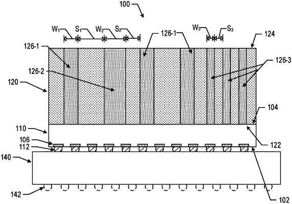
attaching a thermal layer to a back side of a die, wherein the thermal layer comprises a material and a plurality of conductive pathways through the material extending from a front side of the thermal layer to a back side of the thermal layer, and wherein the plurality of conductive pathways include first conductive pathways having a first pitch and second conductive pathways having a second pitch different from the first pitch; and
coupling at least one conductive pathways of the plurality of conductive pathways to the back side of the die by a metal-to-metal interconnect, by a solder interconnect, or by an anisotropic conductive material.