| CPC H01L 23/573 (2013.01) [G04F 1/005 (2013.01); H01L 21/705 (2013.01); H01L 27/013 (2013.01); H01L 27/101 (2013.01)] | 29 Claims |
|
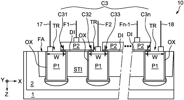
1. An integrated circuit, comprising:
a semiconductor substrate having a front face;
a first trench and second trench extending into the semiconductor substrate from the front face;
a first conductive region housed in each of the first trench and second trench and insulated from the semiconductor substrate by an insulating liner;
a dielectric layer extending over the front face of the semiconductor substrate and further extending at least partially over the first conductive region in the first trench and at least partially over the first conductive region in the second trench;
wherein the dielectric layer has a thickness allowing charge to flow by direct tunneling effect;
a second conductive region on the dielectric layer;
wherein the first conductive region in the first trench, the dielectric layer and the second conductive region form a first capacitor;
wherein the first conductive region in the second trench, the dielectric layer and the second conductive region form a second capacitor connected in series with the first capacitor;
a semiconductor well that is housed in the semiconductor substrate;
a first contact and a second contact which are electrically connected by an electrical path through the semiconductor well, wherein said electrical path comprises a section of said semiconductor well that is located underneath a bottom of the first and second trenches; and
a detection circuit configured to detect an electrical discontinuity in the semiconductor well between the first contact and the second contact.
|