| CPC H01L 23/552 (2013.01) [H01L 21/743 (2013.01); H01L 23/481 (2013.01); H01L 24/05 (2013.01); H01L 24/06 (2013.01); H01L 24/14 (2013.01); H01L 27/1203 (2013.01); H01L 2224/0401 (2013.01); H01L 2224/0557 (2013.01); H01L 2224/09103 (2013.01); H01L 2224/1403 (2013.01)] | 20 Claims |
|
1. An integrated circuit chip comprising:
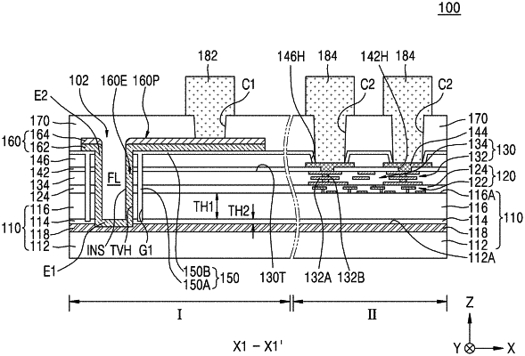
a semiconductor on insulator (SOI) substrate having a structure in which a bulk substrate, a buried insulating film, and a semiconductor body layer are sequentially stacked;
a conductive ion implantation region formed at a position adjacent to the buried insulating film in the bulk substrate;
an integrated circuit portion formed on an active surface of the semiconductor body layer; and
a penetrating electrode portion arranged in a through-via hole at a position spaced apart from the integrated circuit portion in a horizontal direction, the through-via hole penetrating the semiconductor body layer and the buried insulating film in a vertical direction, the penetrating electrode portion connected to the conductive ion implantation region, and the penetrating electrode portion defining an inner insulating space inside the through-via hole,
wherein a vertical distance from the semiconductor body layer to a ground pad portion is greater than a vertical distance from the semiconductor body layer to at least one contact pad, and
wherein a vertical length of a first connection terminal is less than a vertical length of at least one second connection terminal.
|