US 11,721,638 B2
Optically detectable reference feature for processing a semiconductor wafer
Oliver Blank, Villach (AT)
Assigned to Infineon Technologies Austria AG, Villach (AT)
Filed by Infineon Technologies Austria AG, Villach (AT)
Filed on Dec. 18, 2020, as Appl. No. 17/126,743.
Application 17/126,743 is a continuation of application No. 16/279,339, filed on Feb. 19, 2019, granted, now 10,910,318.
Claims priority of application No. 102018103738.4 (DE), filed on Feb. 20, 2018.
Prior Publication US 2021/0104470 A1, Apr. 8, 2021
This patent is subject to a terminal disclaimer.
Int. Cl. H01L 23/544 (2006.01); H01L 21/66 (2006.01); H01L 21/78 (2006.01)
CPC H01L 23/544 (2013.01) [H01L 21/78 (2013.01); H01L 22/20 (2013.01); H01L 2223/5446 (2013.01); H01L 2223/54426 (2013.01)] 20 Claims
OG exemplary drawing
 
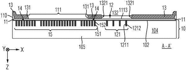
1. A semiconductor wafer, comprising:
a semiconductor body;
an insulation layer on the semiconductor body;
a scribeline region designated to be subjected to a wafer separation processing stage; and
an optically detectable reference feature laterally spaced inward from the scribeline region and configured to be a reference position during the wafer separation processing stage,
wherein the optically detectable reference feature extends into a subsection of an exposed section of the insulation layer.