US 11,721,636 B2
Circuit die alignment target
Anthony M. Fuller, Corvallis, OR (US); Michael W. Cumbie, Corvallis, OR (US); and Chien-Hua Chen, Corvallis, OR (US)
Assigned to Hewlett-Packard Development Company, L.P., Spring, TX (US)
Appl. No. 16/603,821
Filed by HEWLETT-PACKARD DEVELOPMENT COMPANY, L.P., Spring, TX (US)
PCT Filed Apr. 15, 2018, PCT No. PCT/US2018/027690
§ 371(c)(1), (2) Date Oct. 8, 2019,
PCT Pub. No. WO2019/203780, PCT Pub. Date Oct. 24, 2019.
Prior Publication US 2021/0402782 A1, Dec. 30, 2021
Int. Cl. H01L 23/544 (2006.01); B41J 2/175 (2006.01); H01L 21/68 (2006.01)
CPC H01L 23/544 (2013.01) [B41J 2/17546 (2013.01); H01L 21/68 (2013.01); H01L 2223/54426 (2013.01)] 11 Claims
OG exemplary drawing
 
1. A circuit die assembly comprising:
a circuit die comprising:
an outermost circuit layer having electrical transmission routings;
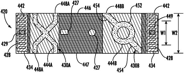
a first alignment target overlying the outermost circuit layer;
a second alignment target formed at or below the outermost circuit layer;
a bond pad region, wherein the second alignment target is within the bond pad region; and
an encapsulant covering the second alignment target while the first alignment target remains uncovered by the encapsulant.