| CPC H01L 23/5386 (2013.01) [H01L 21/486 (2013.01); H01L 21/4846 (2013.01); H01L 21/4853 (2013.01); H01L 21/4857 (2013.01); H01L 23/49811 (2013.01); H01L 23/49822 (2013.01); H01L 23/49827 (2013.01); H01L 23/49838 (2013.01); H01L 23/5381 (2013.01); H01L 23/5384 (2013.01); H01L 23/5385 (2013.01); H01L 23/562 (2013.01); H01L 24/16 (2013.01); H01L 2224/16227 (2013.01); H01L 2924/351 (2013.01)] | 25 Claims |
|
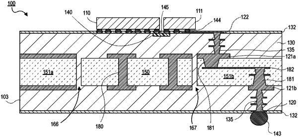
1. A package substrate, comprising:
a core substrate between a first alternate core substrate and a second alternate core substrate, wherein the first alternate core substrate includes a plurality of conductive layers and a plurality of vias, and wherein the second alternate core substrate does not include a conductive layer therein;
a dielectric layer surrounding the core substrate and the first and second alternate core substrates, wherein the dielectric layer is over and under the core substrate and the first and second alternate core substrates;
a first conductive layer on a top surface of the dielectric layer;
a second conductive layer on top surfaces of the core substrate and the first and second alternate core substrates; and
a third conductive layer on bottom surfaces of the core substrate and the first and second alternate core substrates, wherein the plurality of conductive layers are coupled to the plurality of vias within the first alternate core substrate, and wherein the plurality of conductive layers and vias couple the second conductive layer to the third conductive layer.
|