US 11,721,630 B2
Method of forming stacked trench contacts and structures formed thereby
Bernhard Sell, Portland, OR (US); and Oleg Golonzka, Beaverton, OR (US)
Assigned to Intel Corporation, Santa Clara, CA (US)
Filed by Intel Corporation, Santa Clara, CA (US)
Filed on Apr. 18, 2022, as Appl. No. 17/723,309.
Application 17/723,309 is a continuation of application No. 16/985,691, filed on Aug. 5, 2020, granted, now 11,335,639.
Application 16/985,691 is a continuation of application No. 16/382,414, filed on Apr. 12, 2019, granted, now 10,784,201, issued on Sep. 22, 2020.
Application 16/382,414 is a continuation of application No. 15/925,151, filed on Mar. 19, 2018, granted, now 10,297,549, issued on May 21, 2019.
Application 15/925,151 is a continuation of application No. 15/419,141, filed on Jan. 30, 2017, granted, now 9,922,930, issued on Mar. 20, 2018.
Application 15/419,141 is a continuation of application No. 15/220,270, filed on Jul. 26, 2016, granted, now 9,559,060, issued on Jan. 31, 2017.
Application 15/220,270 is a continuation of application No. 14/994,109, filed on Jan. 12, 2016, granted, now 9,437,546, issued on Sep. 6, 2016.
Application 14/994,109 is a continuation of application No. 14/581,498, filed on Dec. 23, 2014, granted, now 9,252,267, issued on Feb. 2, 2016.
Application 14/581,498 is a continuation of application No. 14/284,808, filed on May 22, 2014, granted, now 9,293,579, issued on Mar. 22, 2016.
Application 14/284,808 is a continuation of application No. 12/215,991, filed on Jun. 30, 2008, granted, now 8,803,245, issued on Aug. 12, 2014.
Prior Publication US 2022/0246529 A1, Aug. 4, 2022
Int. Cl. H01L 23/535 (2006.01); H01L 21/768 (2006.01); H01L 23/485 (2006.01); H01L 23/522 (2006.01); H01L 21/28 (2006.01); H01L 29/49 (2006.01); H01L 29/66 (2006.01); H01L 29/78 (2006.01); H01L 21/8234 (2006.01); H01L 23/528 (2006.01); H01L 23/532 (2006.01); H01L 27/088 (2006.01); H01L 29/08 (2006.01); H01L 29/417 (2006.01)
CPC H01L 23/535 (2013.01) [H01L 21/28052 (2013.01); H01L 21/28123 (2013.01); H01L 21/76805 (2013.01); H01L 21/76889 (2013.01); H01L 21/76895 (2013.01); H01L 21/76897 (2013.01); H01L 21/823425 (2013.01); H01L 21/823468 (2013.01); H01L 21/823475 (2013.01); H01L 23/485 (2013.01); H01L 23/528 (2013.01); H01L 23/5226 (2013.01); H01L 23/53257 (2013.01); H01L 23/53266 (2013.01); H01L 27/088 (2013.01); H01L 29/0847 (2013.01); H01L 29/4175 (2013.01); H01L 29/4925 (2013.01); H01L 29/66666 (2013.01); H01L 29/7827 (2013.01); H01L 2924/0002 (2013.01)] 20 Claims
OG exemplary drawing
 
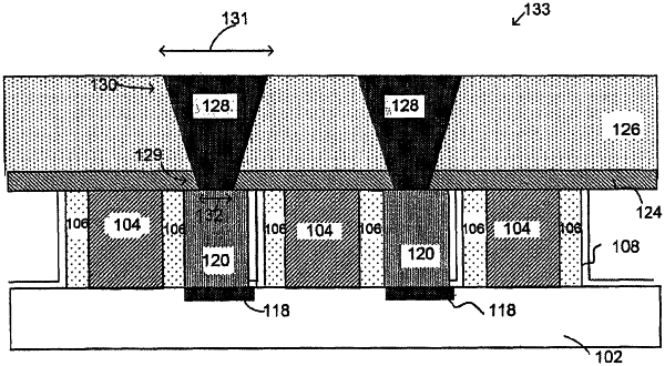
1. An integrated circuit structure, comprising:
a first gate structure;
a second gate structure laterally spaced apart from the first gate structure;
a third gate structure laterally spaced apart from the second gate structure;
a first source or drain region between the first and second gate structures;
a second source or drain region between the second and third gate structures;
a first contact structure over the first source or drain region;
a second contact structure over the second source or drain region;
a third contact structure in contact with the first contact structure, the third contact structure having a top portion wider than a bottom portion;
a first dielectric spacer laterally between the first gate structure and the first contact structure;
a second dielectric spacer laterally between the second gate structure and the first contact structure;
a third dielectric spacer laterally between the second gate structure and the second contact structure;
a fourth dielectric spacer laterally between the third gate structure and the second contact structure; and
a dielectric layer above the first, second and third gate structures, and above at least a portion of the first, second, third and fourth dielectric spacers.