| CPC H01L 23/535 (2013.01) [H01L 21/76805 (2013.01); H01L 21/76816 (2013.01); H01L 21/76877 (2013.01); H01L 21/76895 (2013.01); H01L 23/5226 (2013.01); H01L 23/5283 (2013.01); H10B 41/27 (2023.02); H10B 43/27 (2023.02)] | 16 Claims |

|
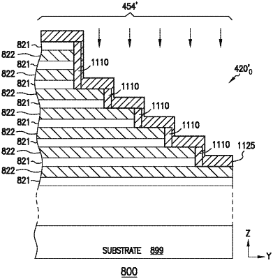
1. A method comprising:
forming levels of first dielectric materials interleaved with levels of second dielectric materials;
forming a staircase structure from the levels of first dielectric materials and the levels of second dielectric materials, such that the levels of first dielectric materials and the levels of second dielectric materials include respective portions that collectively form the staircase structure, wherein the staircase structure includes first regions and second regions coupled to the first regions, the second regions including respective sidewalls;
forming a polysilicon material on the first regions and the second regions of the staircase structure;
doping portions of the polysilicon material on the first regions to form portions of doped polysilicon material on the first regions; and
removing materials from the second regions to separate the portions of doped polysilicon material on the first regions from each other, wherein the materials include at least portions of the polysilicon material formed on the second regions.
|
|
7. A method comprising:
forming levels of first dielectric materials interleaved with levels of second dielectric materials;
forming a staircase structure from the levels of first dielectric materials and the levels of second dielectric materials, such that the levels of first dielectric materials and the levels of second dielectric materials include respective portions that collectively form the staircase structure, wherein the staircase structure includes first regions and second regions coupled to the first regions, the second regions including respective sidewalls;
forming dielectric spacers on sidewalls of the second regions;
forming a polysilicon material on the first regions and on the dielectric spacers;
doping the poly silicon material to form doped poly silicon material; and
removing materials from respective sidewalls of the dielectric spacers to separate at least part of the doped polysilicon material into portions of doped polysilicon material on the first regions, wherein the materials include at least portions of the polysilicon material on the dielectric spacers.
|
|
12. A method comprising:
forming levels of first dielectric materials interleaved with levels of second dielectric materials;
forming a memory cell string including forming a pillar of the memory cell strings through the levels of first materials and the levels of second dielectric materials;
forming a staircase structure from the levels of first dielectric materials and the levels of second dielectric materials, such that the levels of first dielectric materials and the levels of second dielectric materials include respective portions that collectively form the staircase structure, wherein the staircase structure includes first regions and second regions coupled to the first regions, the second regions including respective sidewalls, wherein a portion of each of the first regions and a portion of each of the second regions are part of a level of first material of the levels of first dielectric materials;
forming a polysilicon material on the first regions and the second regions of the staircase structure;
doping portions of the polysilicon material formed on the first regions to form portions of doped polysilicon material on the first regions;
removing portions of the polysilicon from the second regions to separate the portions of doped polysilicon material on the first regions from each other, the portions of doped polysilicon material forming respective conductive pads; and
replacing the levels of first dielectric materials with respective levels of conductive materials, such that the levels of conductive materials contact the conductive pads.
|