| CPC H01L 23/535 (2013.01) [H01L 21/76805 (2013.01); H01L 21/76831 (2013.01); H01L 21/76843 (2013.01); H01L 21/76895 (2013.01); H01L 21/76898 (2013.01); H01L 23/481 (2013.01); H01L 23/485 (2013.01); H01L 23/5286 (2013.01); H01L 29/0653 (2013.01); H01L 29/0847 (2013.01); H01L 29/41791 (2013.01); H01L 29/66795 (2013.01); H01L 29/7851 (2013.01)] | 20 Claims |

|
1. A semiconductor device comprising:
a substrate comprising a first surface and a second surface opposite to each other, and comprising an active region on the first surface and defined by a first isolation region;
a plurality of active fins arranged on the active region, wherein the plurality of active fins extend in a first direction and are defined by a second isolation region having a second depth smaller than a first depth of the first isolation region, wherein the plurality of fins are spaced apart in a second direction that is different from the first direction;
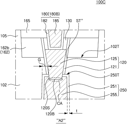
a buried conductive wiring in a trench adjacent to the plurality of active fins, and extending in the first direction, wherein the trench comprises a trench depth extending along a vertical direction that is perpendicular to the first and second directions, and wherein the trench depth is less than the first depth of the first isolation region and greater than the second depth of the second isolation region;
a filling insulation portion in the trench, and comprising the buried conductive wiring therein;
an interlayer insulation layer on the first and second isolation regions and on the buried conductive wiring;
a contact structure penetrating the interlayer insulation layer, and contacting the buried conductive wiring; and
a conductive through structure extending through the substrate from the second surface to the trench, and contacting the buried conductive wiring.
|