| CPC H01L 23/5226 (2013.01) [H01L 23/528 (2013.01); H01L 23/53204 (2013.01)] | 20 Claims |
|
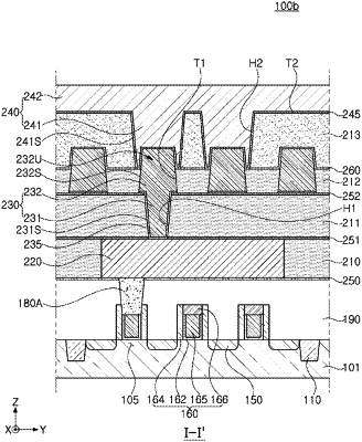
1. A semiconductor device, comprising:
a first insulating layer, a second insulating layer, and a third insulating layer that are sequentially disposed on a substrate;
a first interconnection structure that includes a first via and a first interconnection layer disposed on the first via, wherein the first via penetrates through the first insulating layer, and wherein the first interconnection layer is connected to the first via, protrudes upward from an upper surface of the second insulating layer, and extends in a first direction; and
a second interconnection structure that includes a second via and a second interconnection layer disposed on the second via, wherein the second via penetrates through the third insulating layer, covers an upper surface and a portion of side surfaces of the first interconnection layer, and is wider in a second direction perpendicular to the first direction than the upper surface of the first interconnection layer, and wherein the second interconnection layer is connected to the second via,
wherein the side surfaces of the first interconnection layer are inclined such that a lower portion of the first interconnection layer is wider in the second direction than an upper portion of the first interconnection layer.
|