| CPC H01L 23/5225 (2013.01) [H01L 21/84 (2013.01); H01L 23/5226 (2013.01); H01L 23/5286 (2013.01); H01L 27/1203 (2013.01)] | 20 Claims |
|
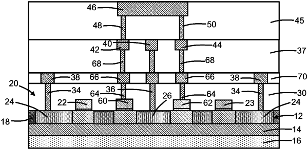
1. A structure comprising:
a field-effect transistor including a first active gate, a second active gate, and a drain region, the drain region positioned in a horizontal direction between the first active gate and the second active gate; and
a back-end-of-line stack including a first metal level and a second metal level over the field-effect transistor, the first metal level including a first interconnect, a second interconnect, and a third interconnect, the second metal level including a fourth interconnect, the third interconnect connected to the drain region, the third interconnect positioned in a vertical direction between the fourth interconnect and the drain region, and the third interconnect positioned in the horizontal direction between the first interconnect and the second interconnect.
|