| CPC H01L 23/49838 (2013.01) [H01L 23/49816 (2013.01); H01L 23/49822 (2013.01); H01L 23/552 (2013.01); H01L 25/105 (2013.01); H01L 24/16 (2013.01); H01L 24/32 (2013.01); H01L 24/73 (2013.01); H01L 2224/16225 (2013.01); H01L 2224/32225 (2013.01); H01L 2224/73204 (2013.01)] | 19 Claims |
|
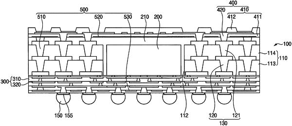
1. A fan-out type semiconductor package comprising:
a frame including a cavity and a middle redistribution layer (RDL) structure configured to at least partially surround the cavity;
a semiconductor chip arranged in the cavity;
a lower RDL structure arranged on the frame and electrically connected with the semiconductor chip and the middle RDL structure;
an upper RDL structure arranged on the frame and electrically connected with the middle RDL structure;
an upper shielding pattern arranged in the upper RDL structure to shield the semiconductor chip from electromagnetic interference (EMI);
a lower shielding pattern arranged in the lower RDL structure to shield the semiconductor chip from the EMI; and
a side shielding pattern arranged in the middle RDL structure to shield the semiconductor chip from the EMI,
wherein the upper shielding pattern and the lower shielding pattern have a thickness of no less than about 5 μm, and the side shielding pattern has a width of no less than about 5 μm,
wherein the side shielding pattern has a stitch via shape including a plurality of cylindrical conductors that are connected to each other by connectors extending along a side surface of the semiconductor chip.
|