| CPC H01L 23/49838 (2013.01) [H01L 23/4985 (2013.01); H01L 24/16 (2013.01); H10K 59/131 (2023.02); H01L 2224/16225 (2013.01)] | 20 Claims |
|
1. A flexible circuit film comprising:
a base film;
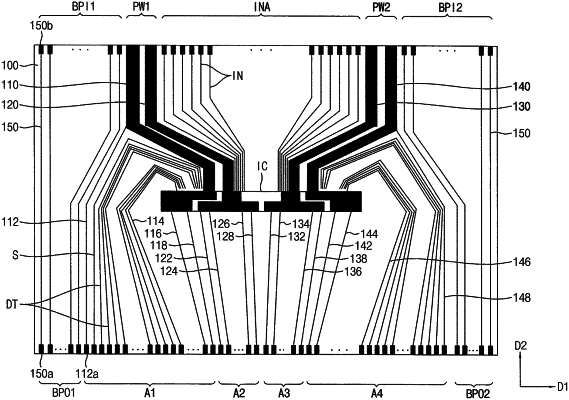
a first power input terminal, a second power input terminal, a first power output terminal set, and a second power output terminal set each disposed on the base film;
an integrated circuit chip disposed between the first power input terminal and the first power output terminal set, disposed between the second power input terminal and the second power output terminal set, and overlapping the base film;
a first power wiring set disposed on the base film, disposed between the first power input terminal and the first power output terminal set, and including a first connection part, wherein the first connection part is disposed between the base film and the integrated circuit chip, is electrically connected to each of the first power input terminal and the first power output terminal set, is not electrically connected to the integrated circuit chip, and overlaps the integrated circuit chip, wherein the first power wiring set further includes a single integral first power input wire and a first power output wire set including multiple power output wires, the first connection part electrically coupling the first power input wire to the first power output wire set; and
a second power wiring set disposed on the base film, disposed between the second power input terminal and the second power output terminal set, and including a second connection part, wherein the second connection part is disposed between the base film and the integrated circuit chip, overlaps the integrated circuit chip, and is spaced from the first connection part in a first direction.
|