| CPC H01L 23/49537 (2013.01) [H01L 21/56 (2013.01); H01L 23/3121 (2013.01); H01L 23/49579 (2013.01); H01L 23/49827 (2013.01)] | 18 Claims |
|
1. A method, comprising:
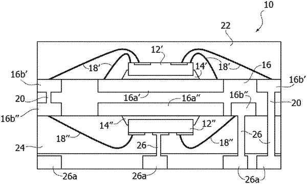
arranging at least one first semiconductor die on a first die pad of a first leadframe structure formed at a first surface of a substrate of laser direct structuring (LDS) material and at least one second semiconductor die at a second die pad of a second leadframe structure formed at a second surface of the substrate of LDS material, the second surface of the substrate being opposite the first surface;
molding package LDS material onto the second surface of the substrate of LDS material, the package LDS material encapsulating the at least one second semiconductor die arranged on the second leadframe structure;
forming in the package LDS material a set of electrical contacts at a surface of the package LDS material opposite the substrate of LDS material;
forming, by applying laser beam processing to the substrate of LDS material and the package LDS material, at least one first electrically-conductive via in the package LDS material, the at least one first electrically-conductive via being at least a portion of an electrically-conductive path between the at least one first semiconductor die and an electrical contact in the set of electrical contacts formed at the surface of the package LDS material opposite the substrate of LDS material;
forming, by applying laser beam processing to the substrate of LDS material, the first leadframe structure at the first surface of the substrate of LDS material and the second leadframe structure at the second surface of the substrate of LDS material.
|