| CPC H01L 23/481 (2013.01) [H01L 21/76838 (2013.01); H01L 21/76898 (2013.01); H01L 23/5226 (2013.01); H01L 23/53238 (2013.01)] | 11 Claims |
|
1. A method for manufacturing a semiconductor structure, comprising:
providing an underlying semiconductor layer;
depositing an insulation layer over the underlying semiconductor layer;
forming a first through semiconductor via extending continuously through the insulation layer;
forming a second through semiconductor via extending continuously through the insulation layer;
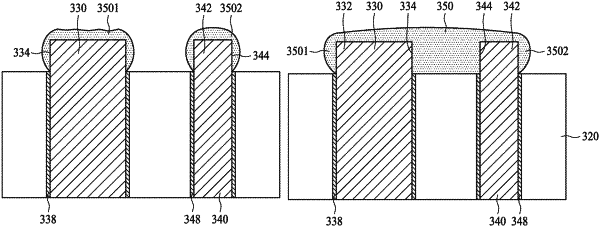
etching a portion of the insulation layer to expose a first upper end of the first through semiconductor via above the insulation layer and a second upper end of the second through semiconductor via above the insulation layer;
depositing an upper conductive metal material directly and laterally connected to a first upper lateral surface of the first upper end and a second upper lateral surface of the second upper end by a self-aligned deposition process, wherein the first through semiconductor via includes copper material, and the second through semiconductor via includes copper material, and the upper conductive metal material includes a conductive copper alloy; and
continuously depositing the upper conductive metal material to form an upper conductive connecting portion to physically and electrically connect the first upper end of the first through semiconductor via and the second upper end of the second through semiconductor via.
|
|
9. A method for manufacturing a semiconductor structure, comprising:
providing an underlying semiconductor layer;
forming a first through semiconductor via extending continuously through the underlying semiconductor layer;
forming a second through semiconductor via extending continuously through the underlying semiconductor layer;
etching a portion of the underlying semiconductor layer from a bottom surface of the underlying semiconductor layer to expose a first bottom end of the first through semiconductor via and a second bottom end of the second through semiconductor via;
depositing a bottom conductive metal material directly and laterally connected to a first bottom lateral surface of the first bottom end and a second bottom lateral surface of the second bottom end by a self-aligned deposition process, wherein the first through semiconductor via includes copper material, and the second through semiconductor via includes copper material, and the bottom conductive metal material includes a conductive copper alloy; and
continuously depositing the bottom conductive metal material to form a bottom conductive connecting portion to physically and electrically connect the first bottom end of the first through semiconductor via and the second bottom end of the second through semiconductor via.
|