| CPC H01L 23/481 (2013.01) [H01L 21/76224 (2013.01); H01L 21/76831 (2013.01); H01L 21/76898 (2013.01); H01L 23/535 (2013.01)] | 20 Claims |
|
1. A method for forming an integrated structure, comprising:
forming a top dielectric layer over a top surface of a substrate;
forming a plurality of vias through the top dielectric layer that extend into the substrate, the plurality of vias being electrically coupled to one another;
forming a bottom dielectric layer on a bottom surface of the substrate;
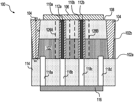
forming an isolation opening and a plurality of contact openings in the bottom dielectric layer and the substrate, the isolation opening passing through the bottom dielectric layer and extending from the bottom surface to the top surface of the substrate, each of the plurality of contact openings having side portions and a bottom portion to expose a respective via of the plurality of vias that is formed in the top dielectric layer;
filling the isolation opening with an insulating layer to form an isolation trench;
filling the plurality of contact openings with a conductive layer to form a plurality of through silicon contacts (TSCs), the conductive layer being in contact with the respective via that is exposed by each of the plurality of contact openings; and
forming a conductive plate over the bottom dielectric layer, the conductive plate being in contact with the plurality of TSCs, the conductive plate being surrounded by the isolation trench and spaced apart from the isolation trench.
|