| CPC H01L 23/367 (2013.01) [H01L 23/5226 (2013.01); H01L 25/0657 (2013.01); H01L 2225/06513 (2013.01); H01L 2225/06589 (2013.01)] | 20 Claims |
|
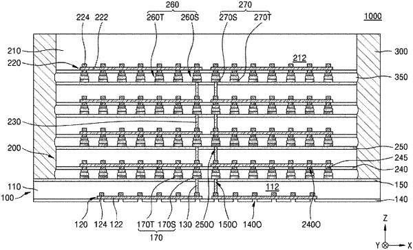
1. A semiconductor package, comprising:
a lower semiconductor chip including a lower semiconductor substrate, a rear surface protecting layer covering a non-active surface of the lower semiconductor substrate, a plurality of lower via electrodes penetrating through the lower semiconductor substrate and the rear surface protecting layer, and a plurality of rear surface signal pads and a plurality of rear surface thermal pads arranged on the rear surface protecting layer;
an upper semiconductor chip including an upper semiconductor substrate, a wiring structure on an active surface of the upper semiconductor substrate, a front surface protecting layer that covers the wiring structure and has a plurality of front surface openings, and a plurality of signal vias and a plurality of thermal vias that fill the plurality of front surface openings, wherein both the plurality of signal vias and the plurality of thermal vias are electrically connected to the wiring structure; and
a plurality of signal bumps connecting between the plurality of rear surface signal pads and the plurality of signal vias, and a plurality of thermal bumps connecting between the plurality of rear surface thermal pads and the plurality of thermal vias, wherein:
the plurality of signal bumps and the plurality of thermal bumps are between the lower semiconductor chip and the upper semiconductor chip, and
the plurality of rear surface signal pads are connected to the plurality of lower via electrodes, and entire bottom surfaces of the plurality of rear surface thermal pads are in contact with the rear surface protecting layer.
|