| CPC H01L 23/3178 (2013.01) [H01L 23/3192 (2013.01); H01L 23/49822 (2013.01); H01L 23/49861 (2013.01)] | 20 Claims |
|
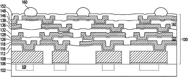
1. A method comprising:
depositing a first metallization pattern on a substrate;
depositing a first insulating layer over the first metallization pattern, the first insulating layer being filler-free;
curing the first insulating layer, causing the first insulating layer to shrink less than 5%;
forming a first opening through the first insulating layer to expose a portion of the first metallization pattern;
without leveling the first insulating layer, depositing a second metallization pattern over the first insulating layer and in the first opening;
depositing a second insulating layer over the second metallization pattern, the second insulating layer being filler-free; and
curing the second insulating layer, causing the second insulating layer to shrink between 20% and 35%.
|