| CPC H01L 23/24 (2013.01) [H01L 21/565 (2013.01); H01L 23/3107 (2013.01); H01L 23/5385 (2013.01); H01L 24/13 (2013.01); H01L 2924/1434 (2013.01); H01L 2924/3511 (2013.01)] | 21 Claims |
|
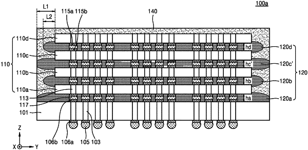
1. A semiconductor package comprising:
a substrate;
a plurality of semiconductor devices stacked on the substrate;
a plurality of underfill fillets disposed between the plurality of semiconductor devices and between the substrate and the plurality of semiconductor devices; and
a single molding resin surrounding the plurality of semiconductor devices and the plurality of underfill fillets,
wherein at least one of the underfill fillets is exposed from side surfaces of the single molding resin,
wherein each of the underfill fillets protrude from side surfaces of the plurality of semiconductor devices.
|