| CPC H01L 22/32 (2013.01) [H01L 22/14 (2013.01); H01L 23/4006 (2013.01); H01L 23/585 (2013.01); H01L 24/20 (2013.01); H01L 24/13 (2013.01); H01L 25/0655 (2013.01); H01L 2224/13024 (2013.01); H01L 2224/221 (2013.01); H01L 2224/2205 (2013.01)] | 20 Claims |
|
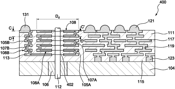
1. A semiconductor device, comprising:
a packaging structure comprising a redistribution layer and a detecting component disposed in the redistribution layer;
a cooling plate over the packaging structure; and
a fixing component penetrating through the packaging structure and the cooling plate, the packaging structure and the cooling plate being fixed by the fixing component,
wherein the detecting component is in a chain configuration having a ring shaped structure circling around the fixing component.
|