| CPC H01L 21/823821 (2013.01) [H01L 21/02532 (2013.01); H01L 21/30604 (2013.01); H01L 21/324 (2013.01); H01L 21/823807 (2013.01); H01L 21/823828 (2013.01); H01L 27/0924 (2013.01); H01L 29/0673 (2013.01); H01L 29/0847 (2013.01); H01L 29/1037 (2013.01); H01L 29/42392 (2013.01); H01L 21/0274 (2013.01); H01L 21/31116 (2013.01); H01L 21/76224 (2013.01); H01L 21/823864 (2013.01); H01L 21/823878 (2013.01); H01L 29/6653 (2013.01); H01L 29/66545 (2013.01)] | 20 Claims |
|
1. A semiconductor structure, comprising:
a substrate;
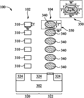
a fin disposed on the substrate, the fin including a source region, a drain region, and a channel region disposed between the source and drain regions, the channel region comprising a plurality of channels vertically stacked over one another, the channels comprising germanium distributed therein;
a gate stack engaging the channel region of the fin; and
gate spacers disposed between the gate stack and the source and drain regions of the fin,
wherein each channel of the channels includes a middle section wrapped around by the gate stack and two end sections engaged by the gate spacers, wherein a concentration of germanium in the middle section is higher than a concentration of germanium in the two end sections, and wherein the middle section further includes a core portion and an outer portion surrounding the core portion and has a germanium concentration profile from the core portion to the outer portion.
|