US 11,721,591 B2
Semiconductor device and method for fabricating the same
Chih-Kai Hsu, Tainan (TW); Ssu-I Fu, Kaohsiung (TW); Chun-Ya Chiu, Tainan (TW); Chi-Ting Wu, Tainan (TW); Chin-Hung Chen, Tainan (TW); and Yu-Hsiang Lin, New Taipei (TW)
Assigned to UNITED MICROELECTRONICS CORP., Hsin-Chu (TW)
Filed by UNITED MICROELECTRONICS CORP., Hsin-Chu (TW)
Filed on Jun. 4, 2021, as Appl. No. 17/338,666.
Application 17/338,666 is a division of application No. 16/807,108, filed on Mar. 2, 2020, granted, now 11,062,954.
Application 16/807,108 is a continuation in part of application No. 15/873,838, filed on Jan. 17, 2018, granted, now 10,607,882, issued on Mar. 31, 2020.
Prior Publication US 2021/0296182 A1, Sep. 23, 2021
Int. Cl. H01L 29/06 (2006.01); H01L 21/8234 (2006.01); H01L 27/088 (2006.01)
CPC H01L 21/823481 (2013.01) [H01L 21/823431 (2013.01); H01L 27/0886 (2013.01); H01L 29/0649 (2013.01)] 5 Claims
OG exemplary drawing
 
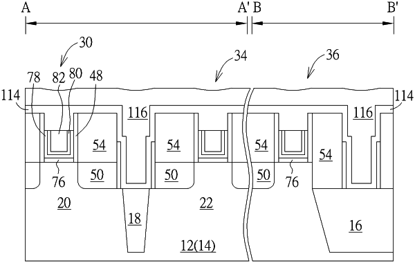
1. A semiconductor device, comprising:
a single diffusion break (SDB) structure dividing a fin-shaped structure into a first portion and a second portion; and
an isolation structure on the SDB structure, wherein the isolation structure comprises a T-shape, a bottom surface of the isolation structure is lower than a top surface of the fin-shaped structure, and the isolation structure further comprising:
a cap layer on the SDB structure, wherein the cap layer is made of a dielectric material; and
a dielectric layer on the cap layer.