| CPC H01L 21/823431 (2013.01) [H01L 21/76224 (2013.01); H01L 21/823412 (2013.01); H01L 21/823481 (2013.01); H01L 27/0886 (2013.01); H01L 29/0653 (2013.01); H01L 29/1095 (2013.01); H01L 29/165 (2013.01); H01L 29/36 (2013.01); H01L 29/66636 (2013.01); H01L 29/7848 (2013.01); H01L 29/7853 (2013.01); H10B 10/12 (2023.02); H01L 21/0217 (2013.01); H01L 21/0223 (2013.01); H01L 21/02057 (2013.01); H01L 21/0257 (2013.01); H01L 21/0262 (2013.01); H01L 21/0274 (2013.01); H01L 21/02164 (2013.01); H01L 21/02255 (2013.01); H01L 21/02271 (2013.01); H01L 21/3081 (2013.01); H01L 21/3086 (2013.01); H01L 21/30604 (2013.01); H01L 21/31053 (2013.01); H01L 29/66545 (2013.01)] | 20 Claims |
|
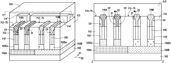
1. A structure, comprising:
a substrate comprising a plurality of doped blocks;
a fin structure disposed on each of the plurality of doped blocks, wherein the fin structure comprises an active channel region and a body region, and an interface exist in between the active channel region and the body region;
dielectric strips physically separating the plurality of doped blocks from one another; and
insulators disposed on the plurality of doped blocks and located in between the body region of the fin structure and the dielectric strips;
strained material portions disposed on the body region of the fin structure, and located on two sides of the active channel region, wherein the strained material portions are in direct contact with the dielectric strips, and a plurality of cavities exist in between the strained material portions and the dielectric strips.
|