| CPC H01L 21/82 (2013.01) [G01R 31/2831 (2013.01); G01R 31/2856 (2013.01); H01L 22/32 (2013.01); H01L 22/34 (2013.01)] | 20 Claims |
|
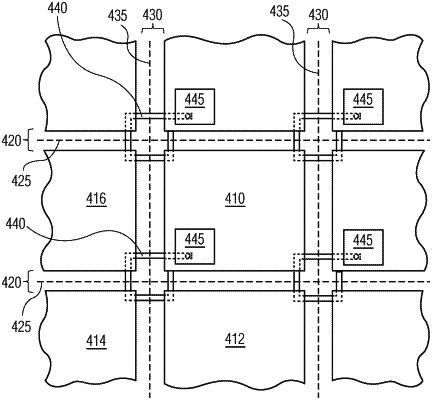
1. A semiconductor wafer having a plurality of semiconductor device die arranged in a grid pattern, the semiconductor wafer comprising:
a first semiconductor device die neighboring a second semiconductor device die, and separated from the second semiconductor device die by a first dicing lane;
a third semiconductor device die neighboring the first semiconductor device die, and separated from the first semiconductor device die by a second dicing lane, wherein the first and second dicing lanes intersect at an intersection region and are substantially perpendicular;
a fourth semiconductor device die, wherein:
the fourth semiconductor device die neighbors the second semiconductor device die, and separated from the second semiconductor device die by the second dicing lane, and
the fourth semiconductor device die neighbors the third semiconductor device die, and separated from the third semiconductor device die by the first dicing lane; and
a first conductor having a continuous shape and coupled to circuitry of the first semiconductor device die, the first conductor comprising:
a first portion of the first conductor extending from the circuitry of the first semiconductor device die at a first side of the first semiconductor device die into the first dicing lane and extending toward the second semiconductor device die, entering the second semiconductor device die at a first side, and extending into a seal ring region of the second semiconductor device die,
a second portion of the first conductor extending from the seal ring region of the second semiconductor device die at a second side of the second semiconductor device die different from the first side of the second semiconductor device into the second dicing lane and extending toward the fourth semiconductor device die, entering the fourth semiconductor device die at a first side, and extending into a seal ring region of the fourth semiconductor device die,
a third portion of the first conductor extending from the seal ring region of the fourth semiconductor device die at a second side of the fourth semiconductor device die different from the first side of the fourth semiconductor device into the first dicing lane and extending toward the third semiconductor device die, entering the third semiconductor device die at a first side, and extending into a seal ring region of the third semiconductor device die, and
a fourth portion of the first conductor extending from the seal ring region of the third semiconductor device die at a second side of the third semiconductor device die different from the first side of the third semiconductor device into the second dicing lane and extending toward the first semiconductor device die, entering the first semiconductor device die, and extending into a seal ring region of the first semiconductor device die,
wherein the first, second, third, and fourth portions of the first conductor together form the continuous shape of the first conductor.
|