| CPC H01L 21/78 (2013.01) [B23K 26/364 (2015.10); H01L 21/673 (2013.01); H01L 21/67739 (2013.01); H01L 23/544 (2013.01); B23K 2101/40 (2018.08); H01L 2223/5446 (2013.01)] | 15 Claims |
|
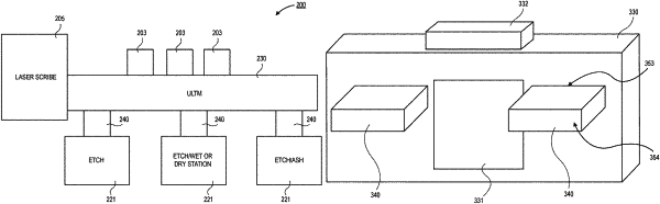
1. A semiconductor processing tool for implementing hybrid laser and plasma dicing of a substrate, comprising:
a transfer module, wherein the transfer module comprises a track robot for handling the substrate;
a first loadlock attached to the transfer module, wherein the first loadlock comprises a first linear transfer system for handling the substrate;
a processing chamber attached to the first loadlock, wherein the first linear transfer system of the first loadlock is configured to insert and remove the substrate from the processing chamber; and
a second loadlock attached to the transfer module, wherein the second loadlock comprises a second linear transfer system for handling the substrate.
|