| CPC H01L 21/76897 (2013.01) [H01L 21/0337 (2013.01); H01L 21/823412 (2013.01); H01L 21/823475 (2013.01)] | 11 Claims |
|
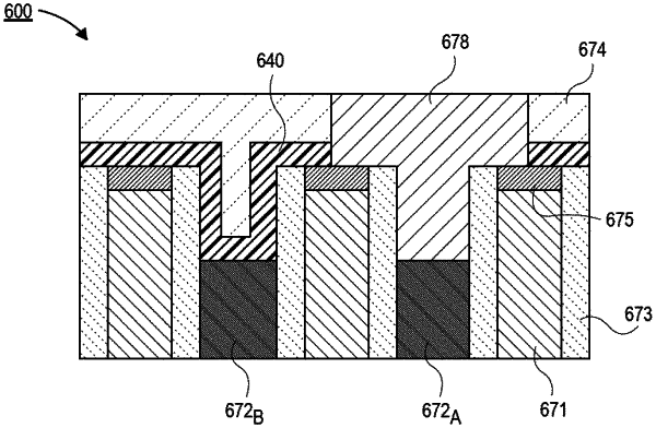
1. A semiconductor device, comprising:
a first interlayer dielectric (ILD);
a plurality of source/drain (S/D) contacts in the first ILD;
a first mask layer on the plurality of S/D contacts;
a plurality of gate electrodes in the first ILD, wherein the plurality of gate electrodes and the plurality of S/D contacts are arranged in an alternating pattern, and wherein top surfaces of the plurality of gate electrodes are below top surfaces of the plurality of S/D contacts so that a plurality of channels defined by sidewall surfaces of the first ILD is positioned over each of the plurality of gate electrodes;
a second mask layer partially filling a first channel of the plurality of channels over a first gate electrode of the plurality of gate electrodes, wherein the first mask layer is vertically between a S/D contact of the plurality of S/D contacts and the second mask layer; and
a fill metal filling a second channel of the plurality of channels over a second gate electrode of the plurality of gate electrodes that is adjacent to the first gate electrode.
|