| CPC H01L 21/76885 (2013.01) [H01L 21/76802 (2013.01); H01L 21/76852 (2013.01); H01L 21/76871 (2013.01); H01L 24/05 (2013.01); H01L 24/13 (2013.01); H01L 24/32 (2013.01); H01L 2224/0231 (2013.01); H01L 2224/0235 (2013.01); H01L 2224/0239 (2013.01); H01L 2224/02331 (2013.01); H01L 2224/0391 (2013.01); H01L 2224/0401 (2013.01); H01L 2224/05008 (2013.01); H01L 2224/05022 (2013.01)] | 20 Claims |
|
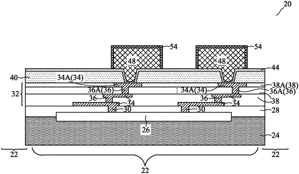
1. A method comprising:
forming a metal seed layer over a first conductive feature of a wafer;
plating a second conductive feature on the metal seed layer, wherein the second conductive feature comprises a top surface and a sidewall surface;
plating a protection layer on the second conductive feature, wherein the protection layer covers the top surface of the second conductive feature, and wherein after the protection layer is formed, a bottommost end of the protection layer is higher than a lower part of the sidewall surface of the second conductive feature; and
removing a portion of the metal seed layer vertically offset from the second conductive feature.
|