| CPC H01L 21/76802 (2013.01) [H01L 21/76877 (2013.01); H01L 23/31 (2013.01); H01L 23/5384 (2013.01); H01L 23/5385 (2013.01); H01L 23/5386 (2013.01); H01L 24/94 (2013.01)] | 20 Claims |
|
1. A semiconductor package comprising:
a lower insulating layer including an under-bump metal layer;
a solder ball on a bottom surface of the lower insulating layer and connected to the under-bump metal layer;
a first substrate on a top surface of the lower insulating layer, the first substrate including a redistribution layer;
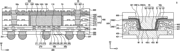
a second substrate including a semiconductor chip electrically connected to the redistribution layer and an interconnection layer, the second substrate having a through-hole exposing the redistribution layer in a region surrounding the semiconductor chip;
a first encapsulation layer covering the second substrate and having a first via hole, the first encapsulation layer filing the through-hole;
a second encapsulation layer covering the first encapsulation layer and having a second via hole in the first via hole, a diameter of the second via hole being less than a diameter of the first via hole;
a via structure filing the second via hole, a sidewall of the via structure having a first surface, a second surface and a third surface, the first surface of the sidewall of the via structure being inclined with respect to a top surface of the second substrate, the second surface of the sidewall of the via structure being inclined with respect to each of the first surface of the sidewall of the via structure, the third surface of the sidewall of the via structure and the top surface of the second substrate, the second surface extending from an end of the first surface to an end of the third surface; and
an upper insulating layer covering a portion of the via structure and a top surface of the second encapsulation layer.
|