| CPC H01L 21/67167 (2013.01) [B08B 3/08 (2013.01); H01L 21/67034 (2013.01); H01L 21/67051 (2013.01); H01L 21/67063 (2013.01); H01L 21/68707 (2013.01)] | 8 Claims |
|
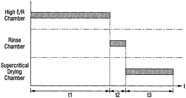
1. A method for manufacturing a semiconductor, the method comprising:
moving a wafer in a high etch rate chamber of a multi-chamber apparatus;
etching silicon nitride of the wafer with a first phosphoric acid solution in the high etch rate chamber;
moving the wafer from the high etch rate chamber to a rinse chamber of the multi-chamber apparatus;
cleaning the wafer with an ammonia mixed solution in the rinse chamber;
moving the wafer from the rinse chamber to a supercritical drying chamber of the multi-chamber apparatus; and
drying the wafer with a supercritical fluid in the supercritical drying chamber,
wherein:
a process time of the high etch rate chamber is a first time,
a process time of the rinse chamber is a second time,
a process time of the supercritical drying chamber is a third time,
a ratio of the first time, the second time, and the third time is 5:1:3, and
a temperature of the ammonia mixed solution is 50° C. to 150° C.
|