|
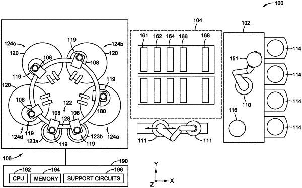
1. A cleaning module comprising: a wafer gripping device configured to support a wafer in a vertical orientation, the wafer gripping device comprising: a catch cup comprising a wall that has an annular inner surface defining a processing region; and a gripper assembly, the gripper assembly comprising: a first plate assembly comprising a plurality of loading pins, each of the plurality of loading pins configured to support an edge of the wafer that is oriented in the vertical orientation; and a second plate assembly comprising a plurality of gripping pins, each of the plurality of gripping pins configured to be: positioned a first distance from a central axis of the wafer gripping device based on the second plate assembly being positioned a second distance in a horizontal direction from the first plate assembly, wherein each of the plurality of gripping pins is configured to contact the edge of the wafer and hold the wafer in the vertical orientation when positioned the first distance from the central axis; and positioned a third distance from the central axis based on the second plate assembly being positioned a fourth distance in the horizontal direction from the first plate assembly, wherein the third distance is greater than the first distance, and the fourth distance is greater than the second distance.
|
