| CPC H01L 21/4846 (2013.01) [H01L 21/486 (2013.01); H01L 21/565 (2013.01); H01L 21/568 (2013.01); H01L 23/3128 (2013.01); H01L 23/3185 (2013.01); H01L 23/498 (2013.01); H01L 23/49838 (2013.01); H01L 24/19 (2013.01); H01L 24/20 (2013.01); H01L 25/105 (2013.01); H01L 25/50 (2013.01); H01L 23/49827 (2013.01); H01L 23/5389 (2013.01); H01L 25/0657 (2013.01); H01L 2224/04105 (2013.01); H01L 2224/12105 (2013.01); H01L 2224/19 (2013.01); H01L 2224/32145 (2013.01); H01L 2224/32225 (2013.01); H01L 2224/48091 (2013.01); H01L 2224/48227 (2013.01); H01L 2224/73265 (2013.01); H01L 2224/73267 (2013.01); H01L 2224/83005 (2013.01); H01L 2224/92244 (2013.01); H01L 2225/0651 (2013.01); H01L 2225/06568 (2013.01); H01L 2225/1035 (2013.01); H01L 2225/1041 (2013.01); H01L 2225/1058 (2013.01); H01L 2924/00 (2013.01); H01L 2924/00012 (2013.01); H01L 2924/00014 (2013.01); H01L 2924/15311 (2013.01); H01L 2924/181 (2013.01); H01L 2924/18162 (2013.01)] | 20 Claims |
|
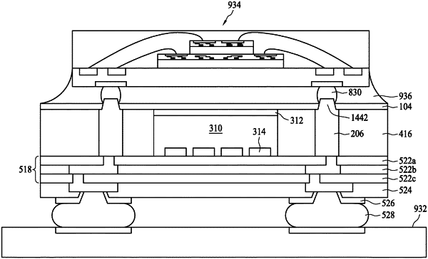
1. A semiconductor device, comprising:
an integrated circuit die;
a molding compound extending along sidewalls of the integrated circuit die;
a conductive structure extending through the molding compound, wherein the conductive structure comprises copper; and
a first insulating layer directly on an upper surface of the molding compound, wherein the conductive structure directly contacts a bottom surface of the first insulating layer, wherein the conductive structure comprises a protrusion extending through the first insulating layer.
|