| CPC H01L 21/0338 (2013.01) [H01L 21/0332 (2013.01); H01L 21/0335 (2013.01); H01L 21/0337 (2013.01)] | 12 Claims |
|
1. A method for forming a semiconductor device, comprising:
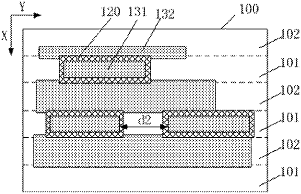
providing a to-be-etched layer including a plurality of first regions and a plurality of second regions, the plurality of first regions and the plurality of second regions being alternatively arranged, and a first region of the plurality of first regions adjoins a corresponding second region of the plurality of second regions;
forming a first mask layer on the to-be-etched layer;
forming a patterned core layer on the first mask layer of the first region;
forming a sidewall spacer material layer on a top surface and a sidewall surface of the core layer and a surface of the first mask layer;
removing the sidewall spacer material layer on the top surface of the patterned core layer;
removing the patterned core layer and the first mask layer at a bottom of the patterned core layer to form a first trench in the first mask layer of the first region;
removing the sidewall spacer material layer on the surface of the first mask layer of a second region;
forming a first patterned layer exposing the first mask layer of the second region; and
using the first patterned layer as a mask to remove the first mask layer of the second region to form a second trench in the first mask layer of the second region.
|