| CPC H01L 21/0274 (2013.01) [H01L 23/16 (2013.01); H01L 23/49822 (2013.01)] | 16 Claims |

|
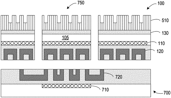
1. A method, comprising:
providing a first semiconductor structure having a first circuit and a first wiring structure formed on a first side thereof;
attaching the first side of the first semiconductor structure to a carrier substrate;
forming a stress film on a second side of the first semiconductor structure;
separating the carrier substrate from the first semiconductor structure;
cutting the stress film and the first semiconductor structure to define at least one chiplet;
bonding the at least one chiplet to a second semiconductor structure that has a second circuit and a second wiring structure such that the second wiring structure is connected to the first wiring structure; and
removing the stress film after the at least one chiplet is bonded to the second semiconductor structure.
|