| CPC H01L 21/02546 (2013.01) [H01L 21/02178 (2013.01); H01L 21/02241 (2013.01); H01L 21/02488 (2013.01); H01L 21/02502 (2013.01); H01L 21/02505 (2013.01); H01L 21/30608 (2013.01); H01L 21/02381 (2013.01); H01L 21/02461 (2013.01); H01L 21/02463 (2013.01)] | 7 Claims |
|
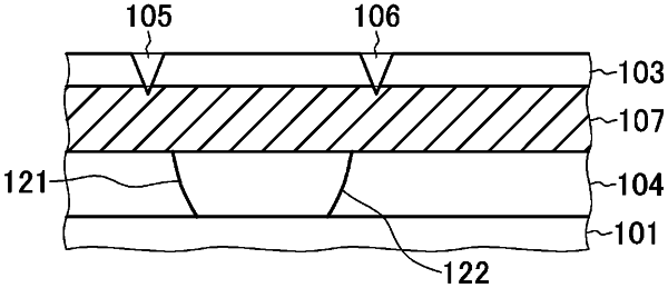
1. A method for forming a semiconductor layer, the method comprising:
(i) crystal-growing, on a substrate, a first semiconductor layer, the first semiconductor layer having a lattice constant in a planar direction of a surface of the substrate which is different from a lattice constant of the substrate in the planar direction of the surface of the substrate;
(ii) crystal-growing a second semiconductor layer on the first semiconductor layer;
(iii) selectively dissolving the second semiconductor layer to form a recess at a dislocation portion of the second semiconductor layer, the recess reaching the first semiconductor layer;
(iv) oxidizing the first semiconductor layer through the recess and forming an insulating film covering a lower surface of the second semiconductor layer; and
(v) crystal-regrowing the second semiconductor layer after forming the insulating film.
|