| CPC H01L 21/02529 (2013.01) [H01L 21/76254 (2013.01); H01L 29/1608 (2013.01)] | 12 Claims |
|
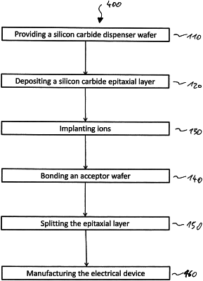
1. A method for manufacturing a silicon carbide device, the method comprising:
providing a silicon carbide dispenser wafer comprising a silicon face and a carbon face;
depositing a silicon carbide epitaxial layer on the silicon face of the dispenser wafer, the silicon carbide epitaxial layer comprising a silicon face facing away from the dispenser wafer;
implanting a designated dopant distribution into the silicon face of the silicon carbide epitaxial layer, wherein the designated dopant distribution is implanted before an acceptor wafer is bonded onto the silicon carbide epitaxial layer;
implanting ions with a predefined energy characteristic to form an implant zone within the silicon carbide epitaxial layer, wherein the ions are implanted with an average depth within the silicon carbide epitaxial layer corresponding to a designated thickness of an epitaxial layer of the silicon carbide substrate being manufactured;
bonding the acceptor wafer onto the silicon face of the implanted silicon carbide epitaxial layer, so that the silicon carbide epitaxial layer is arranged between the dispenser wafer and the acceptor wafer; and
splitting the silicon carbide epitaxial layer along the implant zone, so that a silicon carbide substrate represented by the acceptor wafer with the epitaxial layer having the designated thickness is obtained;
wherein the silicon carbide epitaxial layer is split, so that the epitaxial layer of the silicon carbide substrate with the designated thickness has a carbon face opposite the silicon face onto which the acceptor wafer is bonded,
wherein the designated dopant distribution is disposed at a face of the silicon carbide epitaxial layer with the designated thickness opposite to the carbon face accessible for silicon carbide device fabrication,
wherein the method further comprises manufacturing the electrical silicon carbide device on the carbon face of the epitaxial layer of the silicon carbide substrate, and
wherein the depositing of the silicon carbide epitaxial layer is the only epitaxial deposition step performed between providing the silicon carbide dispenser wafer and manufacturing the electrical silicon carbide device.
|