| CPC H01L 21/02499 (2013.01) [H01L 21/0245 (2013.01); H01L 21/02502 (2013.01); H01L 21/02507 (2013.01); H01L 21/02532 (2013.01); H01L 21/3065 (2013.01); H01L 21/30604 (2013.01); H01L 29/66568 (2013.01)] | 20 Claims |
|
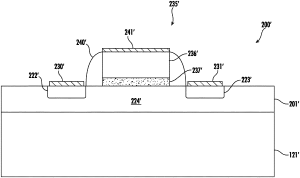
1. A method for making a semiconductor device comprising:
forming a superlattice above a semiconductor layer, the superlattice comprising a plurality of stacked groups of layers, each group of layers comprising a plurality of stacked base semiconductor monolayers defining a base semiconductor portion, and at least one non-semiconductor monolayer constrained within a crystal lattice of adjacent base semiconductor portions;
selectively etching the superlattice to remove semiconductor atoms and cause non-semiconductor atoms to accumulate adjacent the semiconductor layer;
epitaxially growing an active semiconductor device layer above the semiconductor layer and accumulated non-semiconductor atoms after the selective etching; and
forming at least one circuit in the epitaxially grown active semiconductor device layer.
|