| CPC H01L 21/0214 (2013.01) [H01L 21/02164 (2013.01); H01L 21/31056 (2013.01); H01L 21/32155 (2013.01); H01L 21/8258 (2013.01); H01L 21/823814 (2013.01); H01L 29/0649 (2013.01); H01L 29/66545 (2013.01); H01L 29/785 (2013.01); H01L 29/7848 (2013.01); H01L 21/76224 (2013.01); H01L 27/0207 (2013.01); H10B 10/12 (2023.02)] | 20 Claims |
|
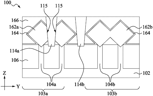
1. A semiconductor structure, comprising:
a substrate;
an isolation structure over the substrate;
a first fin extending from the substrate and through the isolation structure;
a first source/drain structure over the first fin;
a contact etch stop layer over the isolation structure and contacting a first side face of the first source/drain structure; and
a first dielectric structure contacting a second side face of the first source/drain structure, wherein the first side face and the second side face are on opposite sides of the first fin in a cross-sectional view cut along a widthwise direction of the first fin, and the first dielectric structure extends higher than the first source/drain structure.
|