| CPC H01L 21/02109 (2013.01) [C08L 79/08 (2013.01); H01L 23/293 (2013.01); H01L 31/0481 (2013.01); H01L 33/54 (2013.01); C08L 2203/16 (2013.01)] | 14 Claims |
|
1. A process of generating a polyimide based dielectric film on a substrate with conducting metal pattern, comprising:
providing a dielectric film forming composition comprising at least one fully imidized polyimide polymer, at least one cross-linker, and at least one solvent, wherein the at least one cross-linker contains a metal-containing (meth)acrylate; and
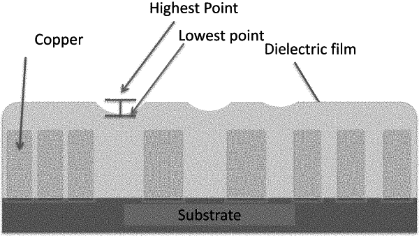
depositing the dielectric film forming composition onto a substrate with conducting metal pattern to form a dielectric film, wherein the difference in the highest and lowest points on a top surface of the dielectric film is less than about 2 microns.
|