| CPC H01L 21/02057 (2013.01) [H01L 21/0273 (2013.01); H01L 21/22 (2013.01); H01L 21/76224 (2013.01)] | 20 Claims |
|
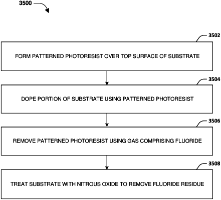
1. A method for forming a semiconductor arrangement, comprising:
forming a patterned photoresist over a top surface of a substrate;
doping a first portion of the substrate using the patterned photoresist;
removing the patterned photoresist using a gas comprising fluoride, wherein fluoride residue from the gas remains on the top surface of the substrate after removing the patterned photoresist;
cleaning the top surface of the substrate;
etching the top surface of the substrate to remove negative oxides after cleaning the top surface of the substrate; and
treating the substrate with nitrous oxide to remove the fluoride residue after etching the top surface of the substrate to remove the negative oxides.
|